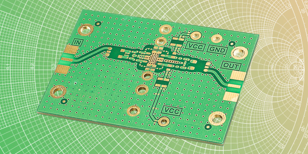
Printed Circuit Boards manufacturing takes place over several steps until the actual PCB is formed. All these processes occur in the PCB factory. Still, before they begin, a design expert or electronic engineer has to develop a design that you can chip in ideas for customization. The form of design varies across industries, whereby some are simple while others are intricate. Despite the introduction of advanced manufacturing technologies and machinery, few errors may develop during the process. The choice of design may be wrong, thus affecting the outcome. We delve into the PCB design selection guide below.
Selection Guideline for a PCB Design
Below are tips to note when choosing a PCB design.
1. Number of PCB layers
Different types of PCBs have a varying number of layers. Knowing the layers enables the manufacturer to know the PCB type plus the design. In addition, the engineer can identify the electrical resistance formed in every layer. They can also tell the reliability and yield required beforehand and choosing the fabrication process is quick. Planning before the start of manufacturing helps lower production costs.
2. Materials of the board
The board is commonly referred to as a base. The PCB base is where all electrical components are attached. The board has a combination of conductive and non-conductive materials necessary for the proper functioning of the PCB. The primary conductive material is copper, which allows current flow from one component to another.
A glass laminated material, FR4 mainly forms the base. It has good mechanical strength needed for support. Being from the glass-epoxy family, it is heat resistant and ideal for live current. High-performance circuits require different materials like PTFE or ceramic bases. They come with fillers for extra support and withstand more power or current.
3. Traces
Traces are essential features in PCB. Manufacturers use various materials to form the traces, but copper is the primary material. Part of the board copper is removed and used to design traces due to its conductive properties. PCB traces possess different qualities and have distinct differences that you should know before settling on a design. Understand how they function to make the selection process manageable.
4. Available parts
PCB designing employs different parts; hence their uses vary. Part selection is important though its time consuming and requires much attention. Know the part you’d like placed on the board or ask the electrical engineer for assistance. The correct parts enhance the PCB quality, minimizes errors, and make it more efficient. Select parts that you can access easily in case of a damage problem. Be keen on the component packaging since it’s used for connection purposes. You can use those with multiple packages to connect several components to the board.
Conclusion
Choosing a PCB design can be tasking. The tips above are straightforward to help you ease the process. Each factor plays a role in the designing steps to produce high-quality PCBs that function correctly in their intended applications. You can also identify which qualities are more important and put more emphasis on them.
